Manufacturing limitations affect the development of products and technologies ranging from pharmaceuticals and health care to energy harvesting, semiconductors and biotechnology — stifling innovation with high costs, small build areas and slow production times.
Researchers at Texas A&M University are seeking to implement a new method of manufacturing 3D nanostructured surfaces consisting of multiple materials by using a high-throughput, high-precision technique.
Dr. Dorrin Jarrahbashi, assistant professor in the J. Mike Walker '66 Department of Mechanical Engineering, is part of a team recently awarded a three-year grant from the National Science Foundation to continue their pursuit of the advancement.
"The created technology can be used in multiple applications and expedite the technological advances in sectors where cost or low-speed production inhibits manufacturing multifunctional nanostructured components," said Jarrahbashi.
Jarrahbashi is working alongside co-principal investigator Dr. Amir Asadi, assistant professor in the Department of Engineering Technology and Industrial Distribution.
"The results from this research will equip multiple U.S. industries with a new scalable manufacturing technique and thus benefit the U.S. economy and society with increased domestic job opportunities and more public access to smart technology," said Asadi.

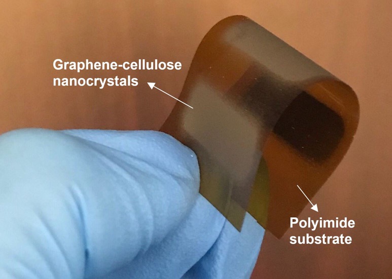
Jarrahbashi said that the team has established a new in-house, spray-deposition manufacturing technique. It uses supercritical carbon dioxide (CO2) to assist with atomization and create very fine and uniform micron-size droplets containing nanoparticles. By engineering the self-assembly of multiple materials inside the deposited droplets, they can fabricate multifunctional, nanostructured components — all without the need for costly preparations or the use of hazardous solvents.
The new process will allow for large-scale, reduced-cost, fast manufacturing of 3D nanostructured surfaces with sizes ranging from a micrometer to a centimeter. Examples of functional coating applications include wearable electronics, smart textiles and paints, antennas and electronic devices.
The use of this new spray deposition technique — along with the combination of multiple materials, including polymer, carbonaceous, and ceramic nanomaterials and tailored patterns — is also expected to enable new levels of multifunctionality.
"Nanostructured surfaces, often fabricated by depositing and patterning nanomaterials on desired substrates, are essential to provide functionalities such as structural, electrical, thermal, magnetic, optical and audio in many devices," Asadi said. "This project supports the development of a manufacturing process that enables scalable and high-precision manufacturing of multifunctional nanostructured surfaces with multiple materials without the need for costly preparations or use of hazardous solvents."
The team is seeking to overcome the challenges of current methods, such as slow and costly treatments and a narrow selection of materials limited by compatibility and small build areas. Their proposed method focuses on the use of nontoxic water, CO2 and pristine nanomaterials that can be integrated into existing manufacturing lines or additive manufacturing stations to integrate large volumes of nanomaterials with high precision.
The team has filed a patent on this developed technology and expects to start a semi-industrial manufacturing line to start producing new sensors based on light filtering and functional coating solutions that address the needs of different industry sectors. They also plan to enhance the current spray system by designing new nozzles for the supercritical, CO2-assisted atomization technique to prepare for scalable manufacturing of multifunctional surfaces.